


Art. 2
Physical isolation of tungsten
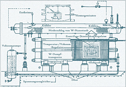
The uniqueness of W as an element is put to good account as follows: its melting point cannot be matched by any other element (including any alloy). So the approach to adopt, for isolation purposes, needs to be based on the melting temperature. This involves converting the element from its fluid state, with the help of precisely applied centrifugal forces, to a nebulous “vapor cloud” of pure W nanoparticles, which are duly precipitated as the desired Tungsten nanopowder. So far, so good. But the technology is much more complex and complicated than just described or as suggested in the greatly simplified image (made in Germany) that refers to the process (otherwise, “anyone” could do it). The complementary values and forces to be applied are determined and combined in numerous mathematical and physical increments. This requires an immense amount of interdisciplinary research work, for which LP has assumed full responsibility.
Art. 3
Basic properties of tungsten

is a refractory metal (from the Latin “refractarius” = stubborn), which belongs to Group 6 (chromium group) of the periodic table (atomic number 74) along with chromium (24) and molybdenum (42) and is therefore classed as a transition metal*(*the term that describes the emergence of unpaired electron spins in the event of partial occupancy of d orbitals, which may – at an atomic level – cause a magnetic moment with para-/ferro-/ferri- and antiferromagnetic behavior). But compared with refractory metals from Group 4 (titanium, zirconium, hafnium), Group 5 (vanadium, niobium, and tantalum), and Group 6 (chromium group) as referred to above, W is the most unique of these. […] This is primarily evident in its extremely high melting point (≤3,423◦C) and boiling point (5,555 °C) (by way of comparison, the temperature at the surface of the sun = 5,700 °C), In respect of the former, it
cannot be beaten by any other element (after carbon, which does not actually melt at all), while its boiling point is only marginally lower than that of rhenium (atomic number 75, so directly next to tungsten, although rhenium is in Group 7, i.e. the manganese group). It does not dissolve in “aqua regia” or *hydrofluoric acid either, but only in a mixture of nitric and *hydrofluoric acid. And there are many more USPs!
For example, thanks to its body-centered cubic lattice structure, tungsten is hardly malleable at all, which means it can only be used in industry if highly specific physicomechanical factors are brought to bear. In this context, the main complementary influence on W’s strength is the degree of purity and formability: the greater (at a correspondingly lower temperature) the degree of deformation, the higher the strength. With a higher degree of formability, grain refinement achieves an increasingly fine grain structure as well as increasing grain boundary areas. This is important because the degree of impurity at grain areas decreases, which in turn increases strength at grain boundaries […]
So to summarize, the higher the impurity at grain boundaries, the “weaker” tungsten will be. It starts to recrystallize from ~1,300◦C, which leads to grain growth and therefore changes in the structure of tungsten itself as well. Recrystallized tungsten, due to changes in grain structure (grain growth), has a correspondingly higher degree of impurity at grain boundaries (i.e. larger grains across a smaller grain boundary area), which duly reduces strength. So until the ductile to brittle transition temperature(DBTT) is exceeded, tungsten is at risk of transgranular fracture as a result of intergranular grain boundary failure. But a higher degree of

purity and deformation (at as low a temperature as possible) can considerably lower the DBTT (±500 °C), which constitutes a KO-criterion: so the thinner, say, tungsten film or wire is, the higher the degree of specific deformation and, therefore, the lower the DBTT will be (including below room temperature if possible, taking any process-specific requirements into account). The most critical variable is the degree of purity. (The above formula is intended as a mathematical analysis module.)
The quality of tungsten owes much therefore to its degree of purity or the proportion of nanocrystals at its inner boundary areas. Polycrystalline solids, with an average grain diameter of <100 nm, start to form at these boundary areas, So the higher this proportion of nanocrystals is, the higher the tensile/breaking strength and abrasion resistance will be too, without impairing ductility. However, the technical usefulness of tungsten in a plastics context is also dependent on a corresponding stabilization of the respective phases within this nanocrystalline structure. For example, if the boundary area in the nanocrystalline state is excessively thick, phase stability will be higher accordingly. In order to determine, in correlative terms, the nanocrystalline structure of tungsten and its phase stability, LP first uses a lateral, high-resolution transmission electron microscope. This gives insights into elements of the nanocrystalline structure (even down to the subnanometer level in some cases) by facilitating so-called nanobeam electron diffraction, which provides identificatory images of tungsten’s crystal lattice structure.
This new application by LP of nanobeam electron diffraction in the context of transmission electron microscopy (see Fig.) can be used to represent diffraction patterns in tiny nanocrystal zones. In other words, LP’s analysis of nanoscale structural elements in tungsten – using the nanobeam electron diffraction technique referred to above – is not practiced anywhere else in the world. One possible reason for this is that the LP methodology (LPM) is uniquely able, thanks to the integrals and differentials used, to perform precise evaluations of irregular nanobeam electron diffraction patterns too (thereby making it possible at all to conduct direct measurements of these

kinds of patterns). Another reason is that LPM supports statistical documentation of highly detailed and accurate grain boundary analysis at nanocrystalline measurement levels.

However, LPM also implies – by way of analogy – that the crystal lattice structure of individual nanoscale structural elements presupposes that the phase transition behavior of tungsten, at nanocrystalline levels, is based on intercomplementary structural properties. This causal relationship, as established by LPM, between the various mechanisms of individual (nanocrystalline) metrics also ultimately makes it possible to optimize precisely those parameters that determine quality – insofar as the individual measurements also always deliver the decisive value for the next stage of the application in each case. Thanks to LPM, it is possible to determine both the structure itself and the individual phases of tungsten, at those nanocrystalline levels, much more precisely than conventional methods have allowed thus far. LPM identificationof the various nanoscale phases, LPM characterizationof phase distribution within the nanocrystalline structure, and LPM analysisof the various orientation relationships
between nanoscale grains and phases make a significant contribution in terms of stabilizing the phases themselves and their transition behavior as regards tungsten in its nanocrystalline state.
So this application of LPM nanobeam electron diffraction, with the help of the transmission electron microscope in question, offers a clear USP insofar as conventional “diffraction analyses” of individual grains are only performed for the purposes of orientation/grain boundary analysis or for phase identification in the context of scanning electron microscopy with electron backscatter diffraction. This also means, however, that the resolution limits for nanoscale structures of tungsten, using conventional measurement methods, are already being reached, based – even under optimal conditions – on a lateral resolution of “only” 30 to 50 nm depending on the material concerned. Not to mention the fact that lateral resolution with conventional electron backscatter diffraction is also impaired by increased defect density, internal tensions, sample drift, or even surface contamination. By contrast, LPM makes it possible to determine diffraction patterns down to 1 nm, i.e. a crystallographic analysis of individual nanograins. The LPM approach to determining the crystallographic orientation of individual nanograins (using nanobeam electron diffraction) offers the following advantages compared with the conventional measurement methods referred to above:
-
Higher lateral resolution due to smaller convergence angle.
-
Less contamination of samples thanks to lower intensity of electron beam.
-
Precise LPM diffraction analysis is possible despite significant deformation of samples as LPM patterns can also be generated in samples with a high defect density, while conventional patterns quickly become smudged and pale.

With LPM evaluation of “diffraction images”, the grains that correlate with the electron beam are geometrically aligned along a crystallographic zonal axis. The resulting diffraction patterns show significant symmetry and are therefore really easy to evaluate. In principle, individual nanograins can be tilted in the direction of the zonal axis by means of a double-tilt holder. For one thing, however, the grains are moved through the field of view during tilting, which also changes their contrast and contours accordingly in the image. But for tungsten at nanocrystalline levels, the respective shift is so big in relation to grain size during tiltingthat tracking of nanoscale grains during tilting can become quite a frustrating experience. Consequently, good diffraction analysis of individual nanograins requires an evaluation of irregular LPM patterns associated with irregularly arranged nanograins. Furthermore, these kinds *of irregular patterns require far more complex evaluation than symmetrical ones – and this is something which can only be done in practice with the help of suitable software. *Thanks to LPM, however, these tend to be the exception. (The image above shows a greatly simplifiedrepresentation of the tilting/evaluation procedure briefly outlined here.)
Art. 4
Integration of W nanopowder into plastic
There are very few options available that allow industry to integrate W nanopowder into plastics. It is indeed possible to mix in or add this powder – which is hard enough to produce in the first place – by means of compounding. But admittedly, this is a rather vague and gimmicky idea as any such procedure might be compared to a manufacturer of pottery, porcelain, or tiles adding “diamond
powder” to its basic mix and hoping this will make the end product “unbreakable”. Throw a stone on it and it shatters …The key, therefore, to sensible integration of our W nanopowder into the compounding process is for this powder to become a woven-in matrix, which is embedded within the plastic like a kind of “wire mesh”. Taking specific account of all expansion coefficients (KO-criterion!), let us assume the W nanopowder is woven as follows: W(II) iodide (WI2–see image on the right). This is obtained by breaking down W(III) iodide or via a halogen exchange reaction from W(II) chloride. In some cases, it can also be obtained by converting W(VI) chloride with hydrogen iodide (at 110 °C, followed by degradation at 500 °C in a vacuum). In my opinion, however, this method is too costly. The recommendation, therefore, would be reversiblemanufacture based on a reaction of I with W, a process which is already known to have proven itself. Another option would be to obtain WI2by

converting W hexacarbonyl with I (depending on the process). Due to intellectual propertyconsiderations, it is not possible here to show any other manufacturing methods or procedures (e.g. how, when melting W, the risk of a transgranular fracture as a result of intergranular grain boundary failure can be averted from a physicomathematical perspective, despite the DBTT being greatly exceeded).
All of the know-how developed is subject to copyright protection (section 106 of the German Act on Copyright and Related Rights (UrhG) and section 78 para. 3(4) of the German Criminal Code (StGB)).
©LP, May 31, 2019